Industry-Specific Laser MicroJet Benefits
The unique water jet guided laser systems offer many advantages for applications in the semiconductor industry compared to conventional diamond blade saws or laser systems.
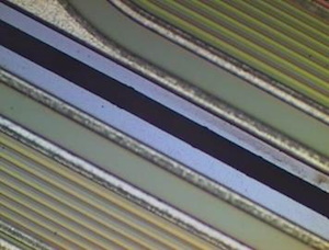
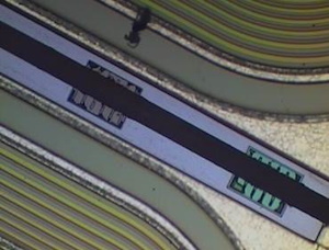
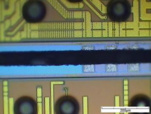
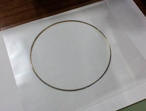
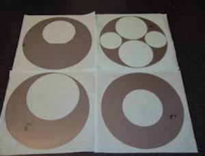
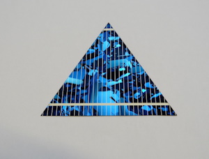
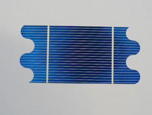
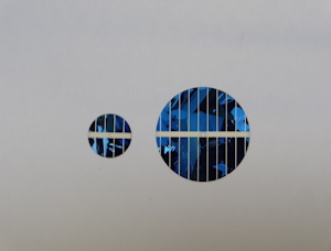
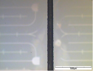
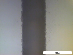
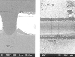
The “gentle” Laser MicroJet (LMJ) method enables the cutting, grooving and dicing of sensitive materials resulting in smooth edges, high wafer fracture strength and less risk of breakage. The flexible LMJ technology allows precise ablation of various semi-conductor materials such as silicon (Si), gallium arsenide (GaAs), silicon carbide (SiC), low-K materials and even coated materials such as Epoxy molded compound wafers of various thicknesses. LMJ machines are able to perform multi-directional 2D-cutting providing engineers with the power to create new chip shapes spanning T-cuts and circular designs with the same quality as standard die patterns.
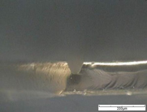
Different laser sources (Green, UV, IR) can be integrated into LMJ systems to tackle future applications. Shinsho LMJ systems are low-cost-of-ownership tools that demand very few consumables and no tool wear. The high-throughput capability especially for thin wafers combined with its nearly damage-free technology (no HAZ, chipping, micro-crack, burr or deposition) allows customers to realize cost benefits by increasing yield.